Description
Accurate AFM Solutions for General Research
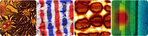
Tall Sample 1.5 µm step height
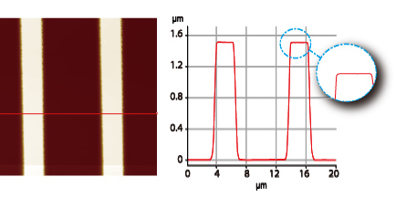
- Scan Mode: Non-contact mode, Topography from Z position sensor
Flat Sample Atomic steps of sapphire wafer
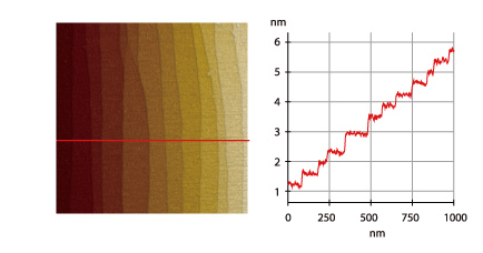
- 0.3 nm step height, Scan Mode: Non-contact mode, Topography from Z position sensor
Hard Sample Tungsten film
- Scan Mode: Non-contact mode, Topography from Z position sensor
Soft Sample Collagen fibril
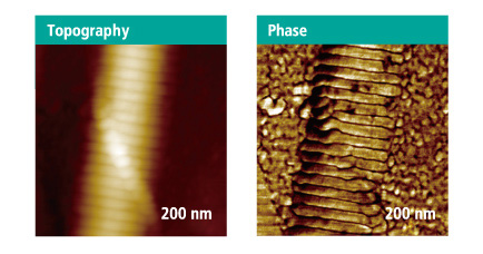
- Scan Mode: Non-contact mode, Topography from Z position sensor
Accurate AFM Measurement with Low Noise Z Detector
Low Noise Z Detector of Park nx10 AFM
- Key technological advance and design feature of NX platform
- Noise level is the lowest in the industry, unmatched by any other
- Used as the default topography signal
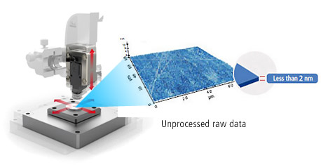
The Z detector is the key technological advance of the new NX-series AFM. It is a new type of strain gauge sensor, innovated by Park. At 0.2 Angstrom, it is the best Z-detector noise in the industry. The noise level is low enough for Z-detector to be used as the default topography signal. If we compare the new NX-series AFM with the previous generation of our AFM model, XE, one can tell the difference. If the Z-detector noise is too high, one cannot clearly observe the atomic steps on the sapphire wafer. The height signal from the Z detector of the Park NX AFM has a noise level, identical to that of the Z-voltage-based topography.
Park NX Series
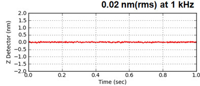 The noise level of the Z position detectors of the Park NX
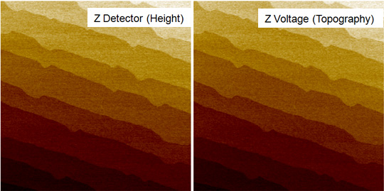 The topography images of a sapphire wafer obtained from nx10
Park XE Series
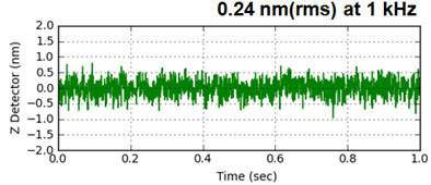 The noise level of the Z position detectors of the Park XE
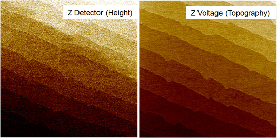 The topography images of a sapphire wafer obtained from XE-100
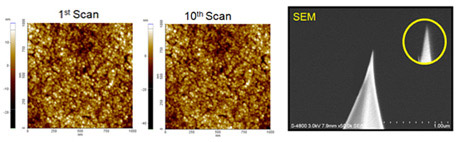
Accurate AFM Scan by True Non-Contact™ Mode
True Non-Contact™ Mode
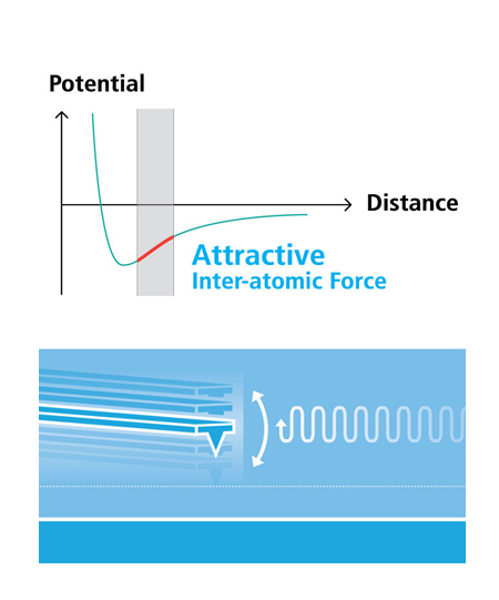
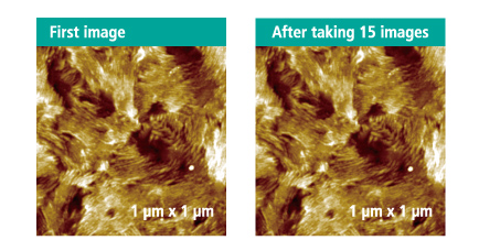
- Less tip wear = Prolonged high-resolution scan
- Non-destructive tip-sample interaction = Minimized sample modification
- Immunity from parameter-dependent results
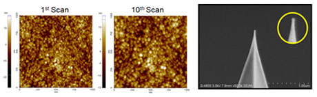
Tapping Imaging
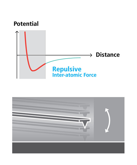
- Quick tip wear = Blurred low-resolution scan
- Destructive tip-sample interaction = Sample damage and modification
- Highly parameter-dependent
The Best User Convenience by Design
Easy Tip and Sample Exchange
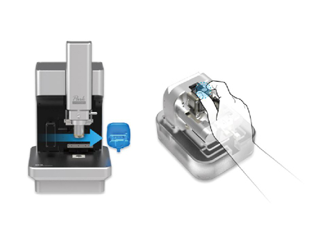
The unique head design allows easy side access allowing you to easily snap new tips and samples into place by hand. The cantilever is ready for scanning without the need for any tricky laser beam alignment by using pre-aligned cantilevers mounted onto the cantilever tip holder.
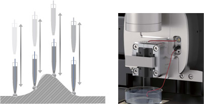
Lightning Fast Automatic Tip Approach
Our automatic tip-to-sample approach requires no user intervention and engages in just 10 seconds after loading the cantilever. By monitoring the cantilever response to the approaching surface, Park NX10 can initiate an automatic fast tip to sample approach within 10 seconds of cantilever loading. Fast feedback by the high-speed Z scanner and low noise signal processing by the NX electronics controller enables quick engagement to the sample surface without any user intervention. It just works, minimal user involvement is required.
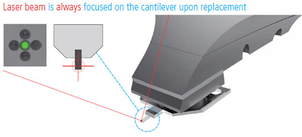
Easy, Intuitive Laser Beam Alignment
With our advanced pre-aligned cantilever holder, the laser beam is focused on the cantilever upon placement. Furthermore, the natural on-axis top-down view, the only one in the industry, allows you to easily find the laser spot. Since the laser beam falls vertically on the cantilever, you can intuitively move the laser spot along the X- and Y-axis by rotating its two positioning knobs. As a result, you can easily find the laser and position it on PSPD using our beam alignment user interface. From there, all you will need is a minor adjustment to maximize the signal to start acquiring the data.
Atomic Force Microscope Surface Analysis & Morphology