Scanning XPS Microprobe

X-ray Photoelectron Spectroscopy (XPS) is the most widely used
surface analysis technique because it can be applied to a broad
range of materials and provides valuable quantitive elemental
and chemical state information from the surface of the material
being studied.
The information XPS provides about surface layers, thin film
structures and interfaces is important for many industrial and
research applications where composition plays a critical role in
performance. It is widely used for polymers, metals, ceramics,
catalysts, thin films, photovoltaics, batteries, wear coatings,
nanomaterials, semiconductor devices, magnetic storage media,
display technology, 2-D materials and biomedical devices.
Physical Electronics (PHI) XPS instruments provide the ability to
obtain spectra with a lateral spatial resolution as small as 10 µm
for the Al K X-ray source.

Request Inquiry

Description

Intuitive Sample Navigation And Confident Analysis Area Identification

  • The unique scanning X-ray microprobe allows SEM like navigation with point-and-click control
  • X-ray induced secondary electron imaging (SXI) provides perfect correlation between imaged areas and spectroscopy

Optimized Depth Profiling

  • Multiple ion gun options (monatomic Ar, C60, argon cluster GCIB) for a variety of organic, inorganic, and mixed materials
  • Full 5-axis stage functionality including rotation/tilt and heating/cooling during sputtering
  • Multipoint profiling within a single sputter crater for on/off defect analysis and precious samples
  • Adjustable solid collection angle for improved angular resolution for Angle Resolved analysis with advanced software for high-throughput film structure analysis

Superior Micro-Area Analysis

  • Highest small area sensitivity on the market
  • <10 microns microprobe size in x and y
  • Image registration for unattended automated micro-area analysis

Suite Of Specialized Solutions For In Situ Characterization Of Advanced Materials

  • Electronic band structure of organic and inorganic materials using UPS, LEIPS, REELS measurement from the same sample location
  • Electrochemical (biasing, polarization studies) experiments
  • Inert sample transfer vessel
  • Fully integrated high energy and high spatial resolution Auger Spectroscopy with elemental mapping at the exact location of interest as XPS

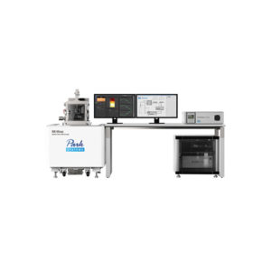
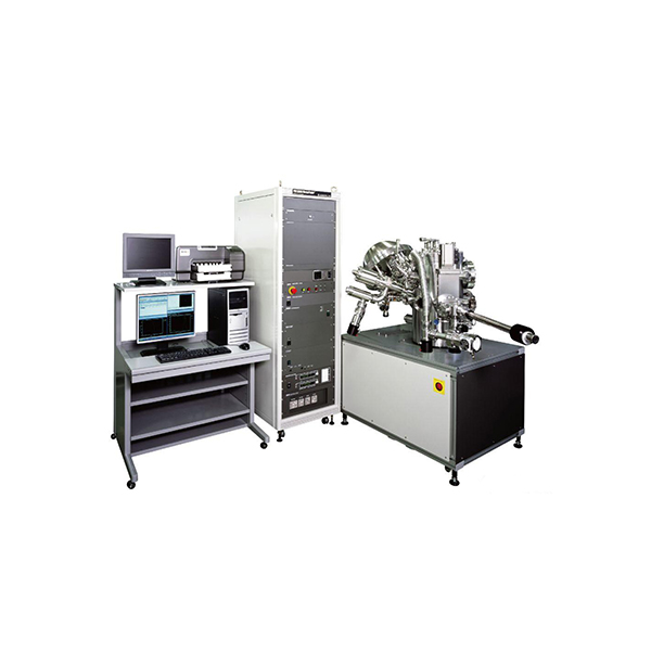
Scanning XPS Microprobe Surface Analysis & Morphology

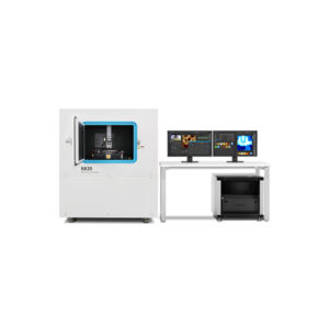
Scanning XPS Microprobe PHI Versa Probe 4

The PHI VersaProbe 4 is a highly versatile, multi-technique instrument with PHI’s patented, monochromatic, micro-focused, scanning X-ray source.  The instrument offers true SEM-like ease of operation with superior micro area spectroscopy and excellent large area capabilities. The fully integrated multi-technique platform of the PHI VersaProbe 4 offers an array of optional excitation sources, sputter ion sources, and sample treatment and transfer capabilities.  These features are essential in studying today’s advanced materials and in supporting your material characterization and problem-solving needs.

The new PHI VersaProbe 4 has improved spectroscopic performance, new large area imaging and mapping capabilities, and environmentally friendly modern configuration with efficient power consumption, faster pump-down and ergonomic design.

Intuitive Sample Navigation And Confident Analysis Area Identification

  • The unique scanning X-ray microprobe allows SEM like navigation with point-and-click control
  • X-ray induced secondary electron imaging (SXI) provides a perfect correlation between imaged areas and spectroscopy
  • NEW X-ray induced Secondary Electron Imaging (SXI) for large-area navigation and large area chemical mapping

Optimized Depth Profiling

  • Multiple ion gun options (monatomic Ar, C60, argon cluster GCIB) for a variety of organic, inorganic, and mixed materials
  • Full 5-axis stage functionality including rotation/tilt and heating/cooling during sputtering
  • Multipoint profiling within a single sputter crater for on/off defect analysis and precious samples
  • Adjustable solid collection angle for improved angular resolution for Angle-Resolved analysis with advanced software for high-throughput film structure analysis

Superior Micro-Area Analysis

  • Highest small area sensitivity on the market
  • <10 microns microprobe size in x and y
  • Image registration for unattended automated micro-area analysis

Suite Of Specialized Solutions For In Situ Characterization Of Advanced Materials

  • Electronic band structure of organic and inorganic materials using UPS, LEIPS, REELS measurement from the same sample location
  • Electrochemical (biasing, polarization studies) experiments
  • Inert sample transfer vessel
  • Fully integrated high energy and high spatial resolution Auger Spectroscopy with elemental mapping at the exact location of interest as XPS