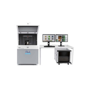
Description
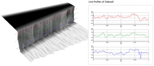
Sidewall measurements for 3D structure study
 The NX20’s innovative architecture lets you detect the sidewall and surface of the sample, and measure their angle. This gives the unit the versatility you need to do more innovative research and gain deeper insights.
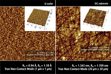
Surface roughness measurements for media and substrates
Surface roughness is one of the key applications where Park NX20 can excel and deliver the accurate failure analysis and quality assurance.
Read More related application
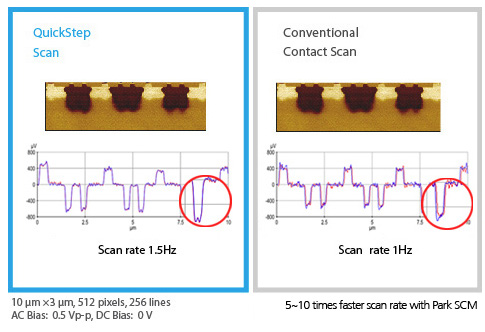
High-resolution electrical scan mode
QuickStep SCM
The Fastest Scanning Capacitance Microscopy
PinPoint AFM
The Frictionless Conductive AFM
Read More related AFM Modes
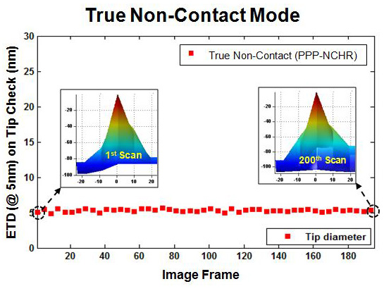
Accurate and Reproducible Measurements for Better Productivity
Tip lifetime performance data on polished silicon wafer: 15,000 scans @ 10Hz using 1 tip!
Reproduce Best AFM Measurement
True Non-Contact Mode preserves the sharp tip end even after imaging 200 images of CrN, so-called tip check sample. CrN has a very abrasive surface that may quickly wear out the sharp tip.
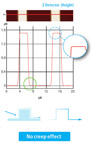
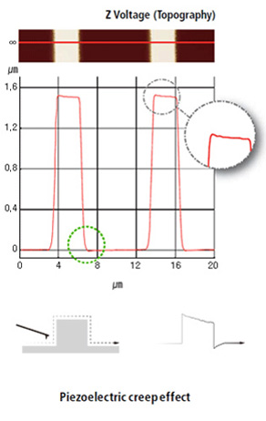
Accurate AFM Topography with Low Noise Z Detector
True Sample Topography™ without piezo creep error
Our AFMs are equipped with the most effective low noise Z detectors in the field, with a noise of .02 nm over large bandwidth. This produces highly accurate sample topography, no edge overshoot and no need for calibration. Just one of the many ways Park AFM saves your time and gives you better data.
- Low noise Z detector signal is used for topography
- Low Z detector noise of 0.02 nm over a large bandwidth
- No edge overshoot at the leading and trailing edges
- Calibration needs to be done only once at the factory
Park NX AFM
Conventional AFM
Atomic Force Microscope Surface Analysis & Morphology
XY Scanner
Single-module flexure XY scanner with closed-loop control Scan range : 100μm x 100μm 50μm x 50μm 25μm x 25μm 20-bit position control and 24-bit position sensor
Stage
XY travel range : 150 mm (200 mm optional) Z travel range : 25 mm Focus travel range: 15 mm Precision encoder for all axes (optional)
Z Scanner
Guided high-force Z scanner Scan range : 15 µm 30 µm 20-bit position control and 24-bit position sensor
Sample Mount
Up to 150 mm (200 mm optional) Vacuum grooves to hold wafer samples
Vision
Objective lens
10× (0.21 NA) objective lens with ultra-long working distance 20× (0.42 NA) objective lens with long working distance and high resolution Direct on-axis vision of sample surface and cantilever Coupled with 10× objective lens (20× optional) Field-of-view: 840 µm × 630 µm CCD: 5 MP
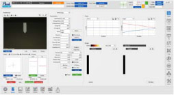
Software
SmartScan™
Dedicated system control and data acquisition software Adjusting feedback parameters in real time Script-level control through external programs(optional)
XEI
AFM data analysis software
Electronics
Signal processing
ADC : 18 channels 4 high-speed ADC channels 24-bit ADCs for X, Y, and Z scanner position sensor DAC : 17 channels 2 high-speed DAC channels 20-bit DACs for X,Y and Z scanner positioning Maximum data size : 4096 x 4096 pixels
Integrated functions
3 channels of flexible digital lock-in amplifier Digital Q control
External signal access
20 embedded signal input/output ports 5 TTL outputs : EOF, EOL, EOP,Modulationand AC bias
AFM Mode (*Optionally available)
Standard Imaging
True Non-Contact Mode PinPoint™ AFM Basic Contact AFM Lateral Force Microscopy (LFM) Phase Imaging Intermittent (tapping) AFM
Electrical Characterization*
Scanning Capacitance Microscopy (SCM) Conductive AFM Electric Force Microscopy (EFM) Piezoresponse Force Microscopy (PFM) Kelvin Probe Microscopy (KPFM)
General Characterization*
Magnetic Force Microscopy(MFM) Scanning Thermal Microscopy(SThM) F-D Spectroscopy Scanning Tunneling Microscopy(STM) Force Modulation Microscopy(FMM) Nanoindentation Nanolithography Nanomanipulation
Options
Customize your AFM to handle any project
Automatic data collection and analysis lets you save time
The NX20 features Park's automation control software that automatically carries out AFM measurements of a sample according to your preset procedure (recipe). It can accurately collect data, perform pattern recognition, and do analysis using its onboard Cognex board and optics module, and export with almost no user in put so you have more time to do innovative research.
Sample Tilting Stage for Sidewall Imaging lets you see more
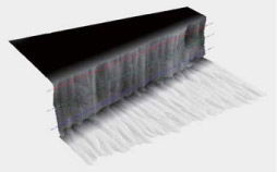
The NX20’s innovative architecture lets you detect the sidewall and surface of the sample, and measure their angle. This gives the unit the versatility you need to do more innovative research and gain deeper insights.
Active Temperature Controlled Acoustic Enclosure Innovative control design allows Park NX20 to quickly reach temperature equilibrium Innovative control design allows Park NX20 to quickly reach temperature equilibrium Park NX20 also features active vibration isolation. Encoders for Motorized Stage • The encoded XY stage travels in 1 µm resolution with 2 µm repeatability • The encoded Z stage travels in 0.1 µm resolution with 1 µm repeatability
Sample Plates • Dedicated small sample holder for electrical measurements • Vacuum grooves to hold wafers • Sample dimension: Up to 200 mm (150 mm default) Cliptype Chip Carrier • Can be used with an unmounted cantilever • Tip bias function available for Conductive AFM and EFM • Tip bias range: -10 V ~ +10 V Precise Temperature Control • Heating & Cooling Stage (0~180 ºC) • 250 ºC Heating Stage • 600 ºC Heating Stage
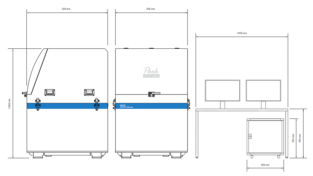
Dimensions in mm


 The NX20’s innovative architecture lets you detect the sidewall and surface of the sample, and measure their angle. This gives the unit the versatility you need to do more innovative research and gain deeper insights.