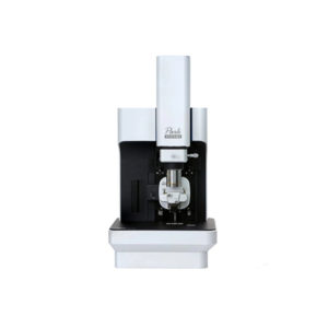
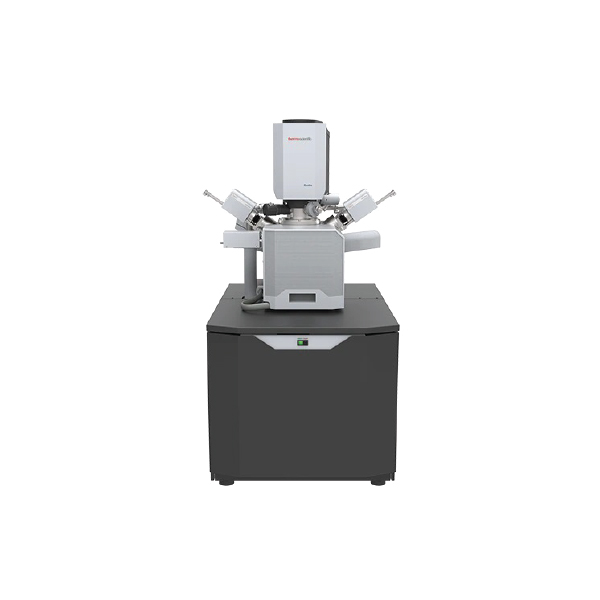
Thermo Fisher Scientific FEI – SEM

scanning electron microscope (SEM) is a type of electron microscope that produces images of a sample by scanning the surface with a focused beam of electrons. The electrons interact with atoms in the sample, producing various signals that contain information about the surface topography and composition of the sample. The electron beam is scanned in a raster scan pattern, and the position of the beam is combined with the intensity of the detected signal to produce an image. In the most common SEM mode, secondary electrons emitted by atoms excited by the electron beam are detected using a secondary electron detector. The number of secondary electrons that can be detected, and thus the signal intensity, depends, among other things, on specimen topography. Some SEMs can achieve resolutions better than 1 nanometer.

Specimens are observed in high vacuum in vacuum or wet conditions in a variable pressure or environmental SEM, and at a wide range of cryogenic or elevated temperatures with specialized instruments.

Request Inquiry

Description

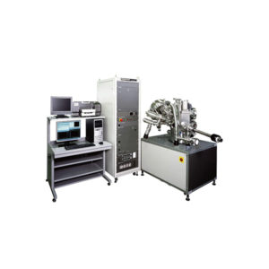
The Thermo Scientific™ SEM is a highly flexible scanning electron microscope (SEM) capable of remarkable all-around performance under a variety of
conditions. With its low vacuum and environmental SEM (ESEM) modes, it is fully equipped to analyze charging, outgassing or otherwise difficult samples.

Highlights
• Easy and quick sample loading for multiple and/or heavy samples
• Simplified sample navigation with the Thermo ScientificTM Nav-Cam™ Camera and navigation montage
• Ease of use thanks to User Guidance and an Undo function
• Excellent image quality with advanced scanning modes and beam deceleration
• Intuitive elemental analysis with Thermo ScientificTM ColorSEM™ Technology
• Compatible with a wide range of samples thanks to dedicated vacuum modes
• Ability to image materials in their natural state with the unique environmental mode
• Easily controlled dynamic experiments with integrated heating/cooling stages
• Wide selection of detectors and accessories including scanning transmission electron microscopy (STEM), cathodoluminescence, scripting, as well as image tiling and stitching


Process control using electron microscopy

Modern industry demands high throughput with superior quality, a balance that is maintained through robust process control. SEM and TEM tools with dedicated automation software provide rapid, multi-scale information for process monitoring and improvement.

Quality control and failure analysis

Quality control and assurance are essential in modern industry. We offer a range of EM and spectroscopy tools for multi-scale and multi-modal analysis of defects, allowing you to make reliable and informed decisions for process control and improvement.

Fundamental Materials Research

Novel materials are investigated at increasingly smaller scales for maximum control of their physical and chemical properties. Electron microscopy provides researchers with key insight into a wide variety of material characteristics at the micro- to nano-scale.

Semiconductor Pathfinding and Development

Advanced electron microscopy, focused ion beam, and associated analytical techniques for identifying viable solutions and design methods for the fabrication of high-performance semiconductor devices.

Yield Ramp and Metrology

We offer advanced analytical capabilities for defect analysis, metrology, and process control, designed to help increase productivity and improve yield across a range of semiconductor applications and devices.

Semiconductor Failure Analysis

Increasingly complex semiconductor device structures result in more places for failure-inducing defects to hide. Our next-generation workflows help you localize and characterize subtle electrical issues that affect yield, performance, and reliability.

Physical and Chemical Characterization

Ongoing consumer demand drives the creation of smaller, faster, and cheaper electronic devices. Their production relies on high-productivity instruments and workflows that image, analyze, and characterize a broad range of semiconductor and display devices.

FEI Microscopic Solution

Environmental scanning electron microscope

The Thermo Scientific Scanning Electron Microscope (SEM) combines a wide array of imaging and analytical modalities with advanced automation to offer the most complete solution of any instrument in its class. It is ideal for industrial research and development, quality control, and failure analysis applications that require high resolution, sample flexibility, and an easy-to-use operator interface. The SEM succeeds the highly successful Thermo Scientific Quanta SEM.

ESEM with EDS

The unique combination of accessible all-round performance, a large set of accessories, and the most intuitive elemental analysis with Thermo Scientific ColorSEM Technology make the SEM the go-to SEM for micro-scale imaging and analysis in any industry or field.

Elemental information at your fingertips

Live composition-based image coloring for intuitive elemental analysis with optional ColorSEM Technology and integrated energy-dispersive X-ray spectroscopy (EDS). Speed up your work and obtain the most complete sample information with always-on analysis.

Excellent image quality

Excellent image quality at low kV and low vacuum thanks to flexible vacuum modes, including through-the-lens differential pumping. Simultaneous secondary electron (SE) and backscattered electron (BSE) imaging in every mode of operation.

Minimize sample preparation time

Low vacuum and SEM capability enable charge-free imaging and analysis of non-conductive and/or hydrated specimens.

In-situ study of materials in their natural state

With the SEM's environmental SEM (SEM) mode, samples can be imaged even if they are hot, dirty, outgassing or wet.

Excellent analytical capabilities

Excellent analytical capabilities with a chamber that allows 3 simultaneous EDS detectors, EDS ports that are 180° opposite, wavelength-dispersive spectroscopy (WDS), coplanar EDS/EBSD, and high-quality charge-free EDS and EBSD in low vacuum.

Easy to use

Easy to use, intuitive software with user guidance and undo functionality makes highly effective operation possible for novice users while enabling experts to do their work faster and with fewer mouse clicks.

The Below Specification is not limited
Resolution
  • 3.0 nm at 30 kV in high vacuum, low vacuum and ESEM
  • 7.0 nm at 3 kV (BSED, beam decel.)
Standard detectors
  • ETD, low-vacuum SED (LVD), gaseous SED for ESEM mode (GSED), IR camera
Optional detectors
  • Thermo Scientific Nav-Cam+ Camera, DBS, DBS-GAD, ESEM-GAD, STEM 3+, WetSTEM, RGB-CLD, EDS, EBSD, WDS, Raman, EBIC, etc.
ColorSEM Technology (optional)
  • Live quantitative SEM image coloring is available based on energy-dispersive X-ray spectroscopy (EDS). Point & ID, linescan, region, element maps and accurate Noran quantification are included.
Stage bias (beam deceleration, optional)
  • -4,000 V to +50 V
Low vacuum mode
  • Up to 2,600 Pa (H2O) or 4,000 Pa (N2)
Stage
  • 5-axis motorized eucentric stage, 110 x 110 mm2 with a 105° tilt range. Maximum sample weight: 5 kg in un-tilted position.
Standard sample holder
  • Standard multi-sample SEM holder uniquely mounts directly
  • onto the stage, hosts up to 18 standard stubs (⌀ 12 mm), does
  • not require tools to mount a sample
Chamber
  • 340 mm inside width, 12 ports, three simultaneous EDS detectors possible, two at 180°, coplanar EDS/EBSD orthogonal to the tilt axis of the stage
In situ accessories (optional)
  • Software controlled -20°C to +60°C Peltier cold stage
  • Software controlled 1,000°C low vacuum/ESEM heating stage
  • Software controlled 1,100°C high vacuum heating stage
  • Software controlled 1,400°C low vacuum/ESEM heating stage
  • Integrated gas injection: up to 2 units (other accessories may limit number of gas injection systems (GIS) available) for beam-induced deposition of the following materials:
    • Platinum
    • Tungsten
    • Carbon
  • Manipulators
  • Cryo-stage
  • Electrical probing / multi-probing stations
Software options